OpenRISC SoC Practical Session Instructions
This session will demonstrate how to get an OpenRISC system up and running. We will compile a pre-configured OpenRISC-based SoC under the FuseSoC environment for the Altera DE0 Nano FPGA board, program the board, and connect to the design with a debugger to download a program before running it.
This guide will
- introduce to OpenRISC and SoC development
- indicate the required set up (source, tools)
- show how to simulate the system
- show how to build the SoC and program the SoC onto the FPGA board
- detail connecting to the SoC via a debugger, downloading and executing code
What is the OpenRISC project?
The OpenRISC project deals with architecture and implementation and tools development. Think of the architecture side as the instruction set manuals, the implementation side the model code (RTL, C, SystemC). The tools are things like the GNU compiler/debugger tool chain and chip debugger.
A SoC?
The synthesisable models we develop aren't much fun (or use) on their own. So we then integrate our synthesisable models into larger systems - a System on (a) Chip (SoC). When they are brought together with peripheral controllers (eg. I2C, SPI, Singlewire) and communications I/O (GPIO, UART, Ethernet, PCIE, etc.) and system infrastructure (memory, debug, interconnect) we then have a system which is capable of many things. Typically the "brains" of the system is the programmable CPU.
An OpenRISC SoC?
In the OpenRISC's case, these CPUs are relatively low-performance embedded-class processors. In an FPGA implementation we can run them up to 100MHz, and they execute up to a single instruction per cycle. However, in certain configurations they are capable of running full operating system kernels like Linux. They are more suited, however, to running embedded real-time operating systems (RTOS).
The OpenRISC 1000 architecture (OR1K or or1k) has a 32-bit instruction word and either 32 or 64-bit data. It it a reduced instruction set computer (RISC) meaning its instructions are relatively simple like:
add register 3 with register 6 and store in register 8
or
load the data at the memory address held in register 4 into register 5
In contrast, a more complex instruction set computer might be capable of doing much more in a single instruction word:
load the data at the memory address in register 2, increment it, compare with zero, and store back at the address held in register 3 while incrementing both registers 2 and 3
This should indicate something rather obvious, which is that the latter seems a lot harder to implement than the former. This means implementations of RISC computers require less logic, and the idea is that the complexity is offloaded onto the software compiler.
The OpenRISC project is lucky enough to have a good quality GNU tool chain port, and an LLVM port also exists. This allows us to compile C and C++ to OpenRISC 1000 machine code and execute it on our models. We also have software libraries in newlib (for baremetal) and uClibc (for Linux userspace, an EGLIBC port is in the works I believe), and the GNU debugger (GDB) which understands the OR1K architecture.
The SoC's CPU core is the mor1kx. It is written in Verilog and provides a choice between 3 major variants, based on the pipeline architecture. They are the 3-stage pipeline espresso core, the 3-stage delay-slot-free pronto espresso core, and the 6-stage cappuccino core which can optionally have MMUs and caches, making it capable and powerful enough to run Linux.
There are several components which must be available for us to do this.
[See the tools install guide page for all of the details] (https://github.com/embecosm/chiphack/wiki/OpenRISC-tools-install)
We can simulate the RTL of the SoC with Icarus and view its internals.
We will run a technology-generic SoC build of the espresso mor1kx core.
cd boards/generic/mor1kx-espresso/sim/run
make rtl-test VCD=1
This will run a simulation, and the VCD=1 option will create a file known as a value change dump which records the status of every signal in the design for viewing afterwards.
If everything went OK you should see:
- Starting simulation of ORPSoC RTL.
- Test: or1k-basic
- VCD in ../out/or1k-basic.vcd
VCD info: dumpfile ../out/or1k-basic.vcd opened for output.
report(0x8000000d);
exit(0x00000000);
The report() functions lines are software indicating status. In this case it has sent the value 0x8000000d, or a hexadecimal pseudo-representation of GOOD. The exit code is 0 meaning no errors.
The software run by the processor in this test is in mor1kx-dev-env/sw/tests/or1k/sim/or1k-basic.S. It a test of a lot of basic instructions such as flag setting, jumping and arithmetic.
The results of the test are in the directory called out/ parallel to the run/ directory.
A trace of the processor's execution is created for each test, too. Inspect it with the following command
less ../out/or1k-basic-trace.log
The line has the format of an 'S' or 'U' to indicate whether the processor is in supervisor or user mode, the program counter (32-bits), the instruction for that PC (32-bits) the disassembly of the instruction, the result if any, and the status of the flag bit.
This pipeline has a delay slot which means that each jump or branch instruction will have its following instruction also executed before the branch is taken. The mor1kx's pronto espresso core does not use this delay slot behaviour.
We can load the VCD of the run with the following:
gtkwave ../out/or1k-basic.vcd
Once it has loaded we can navigate the hierarchy of the design. Expand the orpsoc_testbench and select the dut or design under test. Type in i_or12 to the Filter box and select those that come up and click Insert to add them to the waveform.
Use the plus and minus buttons to zoom in and out - at the beginning of a simulation signals are usually X which means undefined. They will not take a value until their reset condition has been met (an edge of the reset signal).
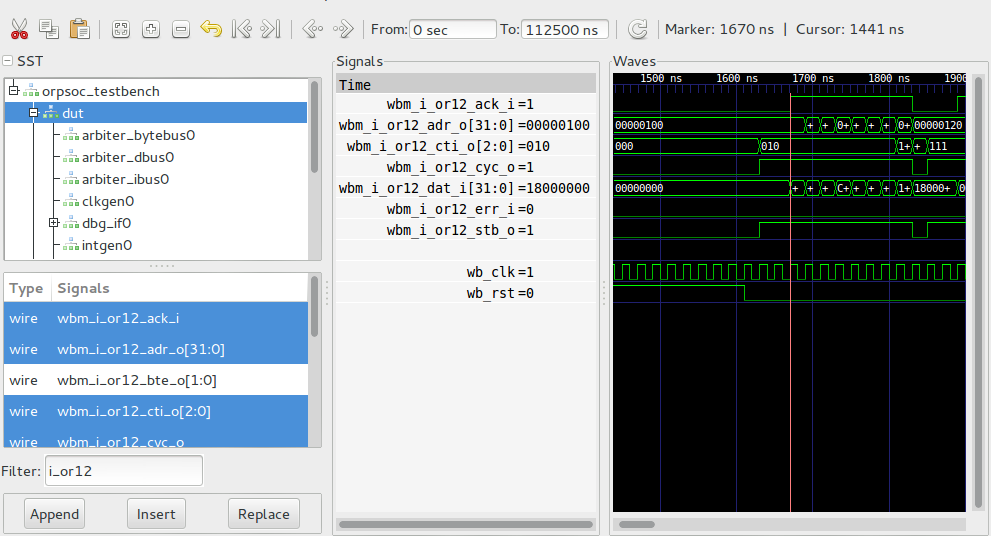
Here we can see the system being taken out of reset (wb_rst going from 1 to 0) and the processor starting to fetch from its reset address 0x100.
The bus interface (Wishbone bus protocol) is bursting in instructions from the memory, and we can see the first instruction request being acknowledged, or acked, by the bus slave and the address begins to change for the next instruction.
Zooming out further shows the behaviour of the bus over a greater a mount of time, indicating just how much is going on in a simple test.
We can run arbitrary tests by specifying TEST=<testname> at runtime. For example, we can run the simplest test, or1k-simple like so:
make rtl-test TEST=or1k-simple VCD=1
The software run by the processor in this test is in mor1kx-dev-env/sw/tests/or1k/sim/or1k-simple.c. It is just a C main() function. The C-runtime setup code is in mor1kx-dev-env/sw/drivers/mor1kx/crt0.S, an OR1K assembly file.
We can modify this file to printf something to the screen during simulation.
Open up the mor1kx-dev-env/sw/tests/or1k/sim/or1k-simple.c file and add the following:
#include "printf.h"- In the main loop do:
- printf("Hello World from the OpenRISC!\n");
The code should look something like this:
#include "cpu-utils.h"
#include "printf.h"
int main()
{
printf("Hello World from the OpenRISC!\n");
report(0x8000000d);
return 0;
}
Now re-run the test with:
make rtl-test TEST=or1k-simple
And we will see the hello world!
Note: The mechanism to get the characters to the console is not a simulated UART in this case, rather a method of signalling the characters to print to the simulator and the testbench code then simply prints the character using the Verilog $print() function.
We can now simulate a hello world over the UART. Add the following to or1k-simple.c:
-
#include "uart.h"and#include "board.h"before the printf include - call
uart_init(0);as the first thing inmain()
eg.:
#include "cpu-utils.h"
#include "board.h"
#include "uart.h"
#include "printf.h"
int main()
{
uart_init(0);
printf("Hello World from the OpenRISC via UART!\n");
report(0x8000000d);
return 0;
}
Run the test again:
make rtl-test TEST=or1k-simple
It will take a lot longer, as it's simulating the UART transmitting at 115200 baud.
Running and generating the VCD:
make rtl-test TEST=or1k-simple VCD=1
We can then look at the UART lines, and the processor's data accesses to the UART core over the bus.
This may take a little while to run on slower PCs
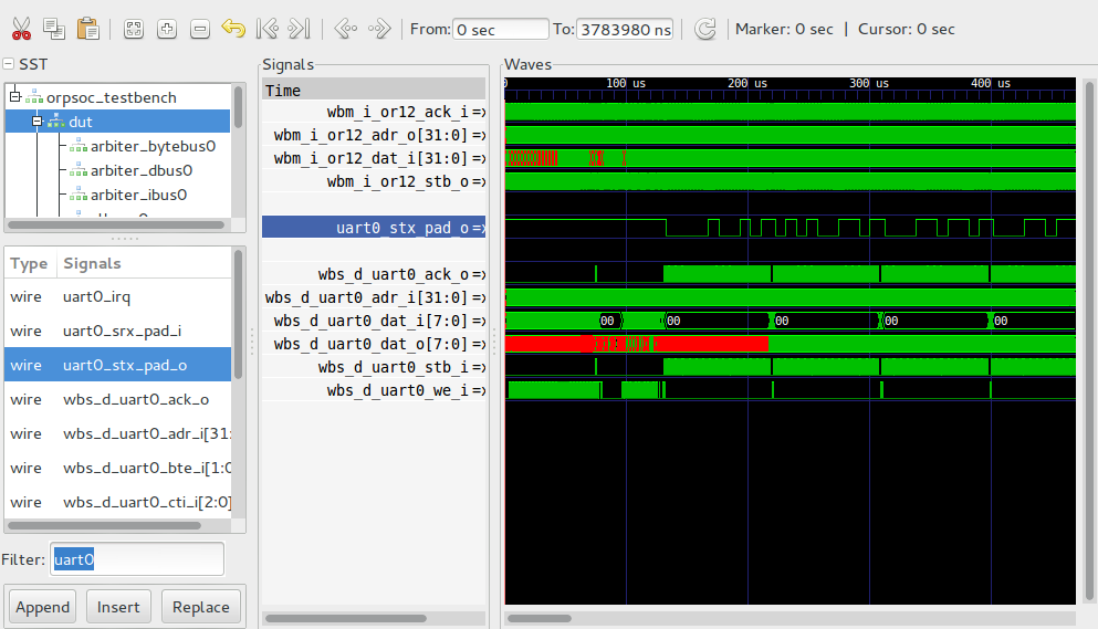
We can see the UART TX line (uart0_stx_pad_o) and the Wishbone interface to the UART peripheral - a lot of accesses are going on as the processor is polling the core to determine when the last byte has been transmitted.
We can, instead, run an example of the UART transmitting with interrupts. Run the software which already exists to demonstrate this:
make rtl-test TEST=uart-txinterrupt VCD=1
The software for this test is in mor1kx-dev-env/sw/tests/uart/sim/uart-txinterrupt.c.
Inspecting the VCD we get:
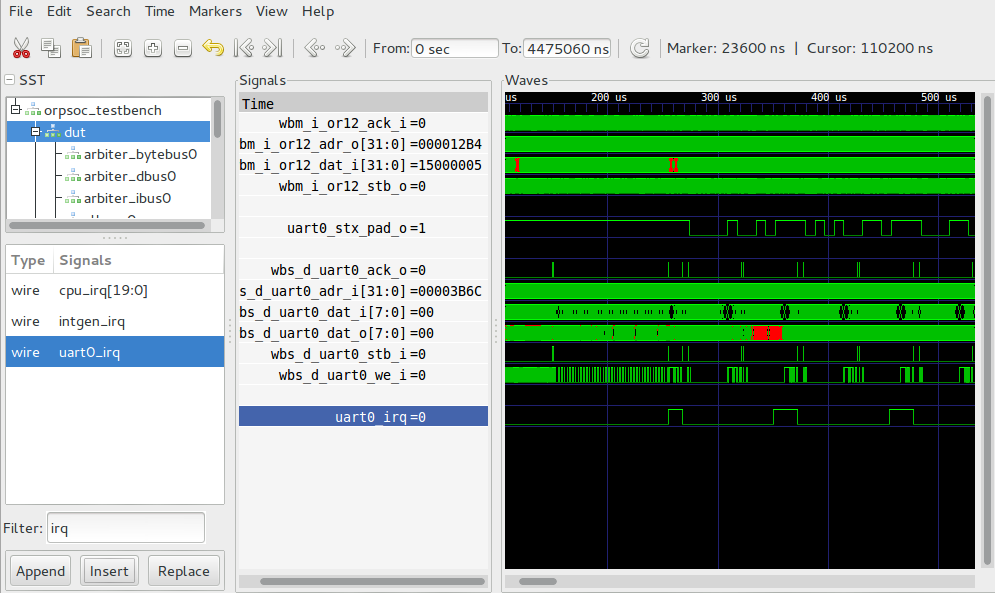
We can see much less activity on the UART's bus interface (the ack signal is no longer thrashing), and the IRQ line is now visible indicating when it finishes each character.
The next section will focus on building and running the system on the DE0 Nano.
The DE0 Nano source is under the mor1kx-dev-env/boards/altera/de0_nano
To synthesise the design using the Quartus tools we want to go into mor1kx-dev-env/boards/altera/de0_nano/syn/quartus/run
First it's best to clean everything:
make clean clean-sw
Here we simply run:
make asm
This will work as long as the $ALTERA_PATH is configured correctly.
This will generate an orpsoc.sof file which cna be programmed onto the board
In the synthesis directory, there is also a makefile recipe for programming the board:
make pgm
One of several things could go wrong here.
- One is that the JTAG daemon running needs to be killed and the Altera one run instead, to do this run:
killall jtagd
sudo /opt/altera/12.1sp1/quartus/bin/jtagd
-
Another problem might be that the OpenOCD debugger is still using the JTAG/USB port - exiting OpenOCD will fix this
-
Another could be basic permissions on the USB device, and running
sudo make pgmmay fix things
From within the OpenOCD directory (presumably $HOME/or1k/openOCD) run:
sudo ./src/openocd -f ./tcl/interface/altera-usb-blaster.cfg -f altera-dev.tcl
You should then see something like:
Info : JTAG tap: or1k.cpu tap/device found: 0x020f30dd (mfg: 0x06e, part: 0x20f3, ver: 0x0)
(ignore any warnings or errors about the JTAG tap...)
target state: halted
Chip is or1k.cpu, Endian: big, type: or1k
Once the proxy is connected we can then connect to it with GDB.
Note that when the proxy connects it will stall the processor.
In a new terminal run the OR1K port of the GNU debugger (GDB).
or1k-elf-gdb
Now connect to the port the proxy is running on:
(gdb) target remote :50001
You should see something like the following:
Remote debugging using :50001
0x00000700 in ?? ()
You can now access the system memory and registers.
Read memory with x <addr> eg:
(gdb) x 0x0
0x0: 0x00000000
See this table of GDB commands for further information.
We can compile software and load software from within GDB.
Some software we can run on the board to flash the LEDs is in the board's sw/tests/gpio/board directory:
(gdb) cd ~/or1k/mor1kx-dev-env/boards/altera/de0_nano/sw/tests/gpio/board/
(gdb) make gpio-blink.elf
Now tell GDB to use this compiled binary:
(gdb) file gpio-blink.elf
Download the file to the system's memory
(gdb) load
This will also set the CPU's program counter (PC) to point to the start address
Finally - run the program!
(gdb) c
....
Press ctrl+c to stall the processor and regain control of the GDB console.
Now build and load the gpio-int test to demonstrate a pushbutton triggering an interrupt:
(gdb) make gpio-int.elf
(gdb) file gpio-int.elf
(gdb) load
(gdb) c
Now press pushbutton 1 (marked KEY1) on the board to toggle an LED. Actually we are doing edge detection in the GPIO peripheral core. On the button being pressed we then install an interrupt handler for when it is released.
(gdb) cd ~/or1k/mor1kx-dev-env/boards/altera/de0_nano/sw/tests/simple_spi/board/
(gdb) make simple_spi-adxl345.elf
(gdb) file simple_spi-adxl345.elf
(gdb) load
(gdb) c
This software is communicating with the ADXL345 accelerometer and reading the X, Y and Z axis acceleration readings, determining which is greatest (and therefore, when at rest, perpendicular to earth's gravity).
LEDs 0 = X (positive)
LEDs 1 = Y (positive)
LEDs 2 = Z (positive)
LEDs 3 = X (negative)
LEDs 4 = Y (negative)
LEDs 5 = Z (negative)
(gdb) make simple_spi-adxl345fancy.elf
(gdb) file simple_spi-adxl345fancy.elf
(gdb) load
(gdb) c
Now double-tap the top of the board with a pen to see the LED pattern switch.